Hello,
I just tried Dejitter 1.3 on a SNES PAL 1Chip with the SuperCIC PCB and WITHOUT RGB Bypassed mod but after plugging it (with original cable of SNES PAL), The fuse blew 🙁
Here is the wiring below :
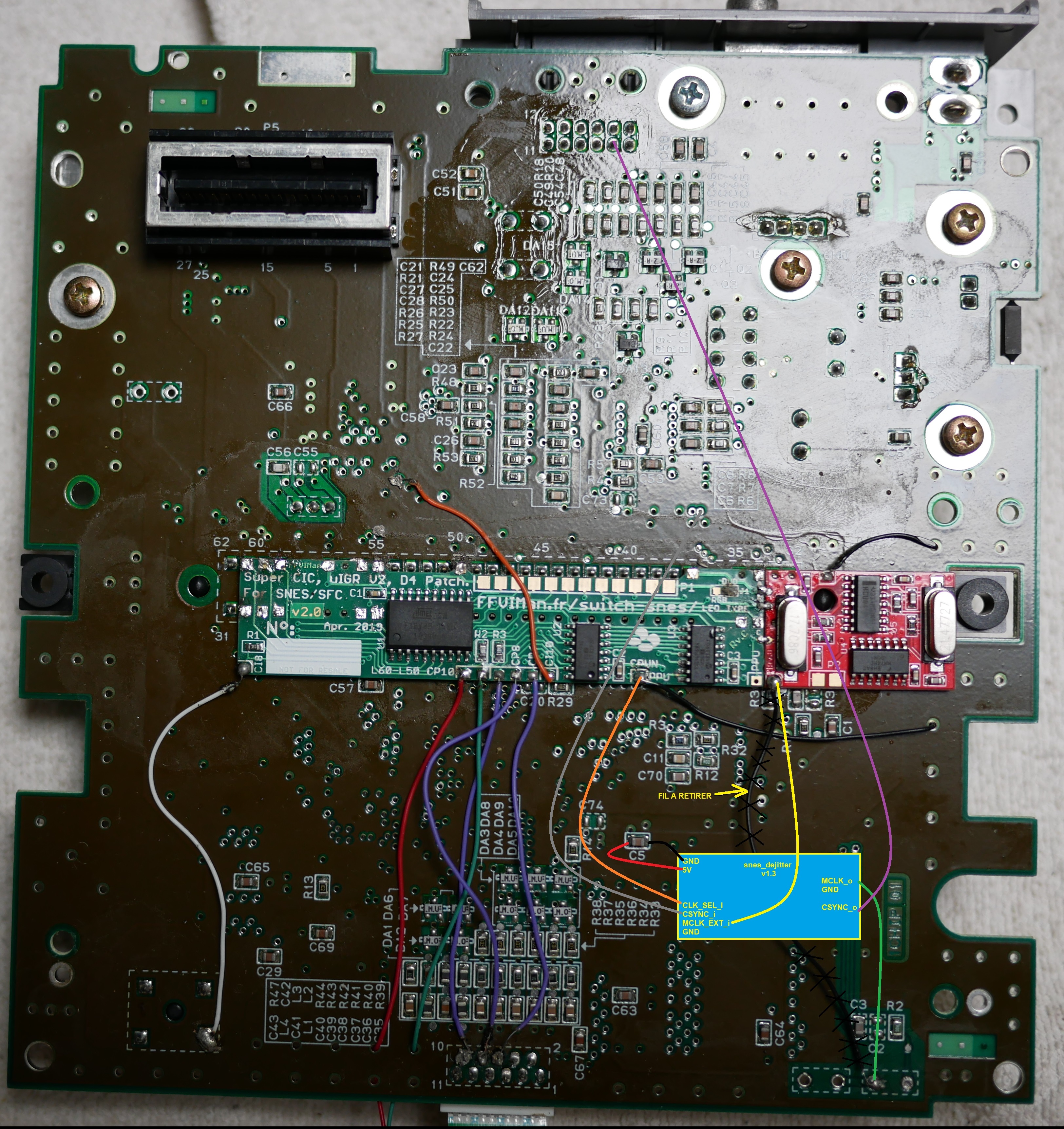
5V and GND from C5.
MCLK_EXT_i from SCIC clock output
CSYNC_i from pin 7 of S-RGB chip or any via connected to that pin.
MCLK_o from left hand through hole of X1 (TC1+)
CLK_SEL_i from SCIC mode pin
But for CSYNC_o, i am a little confused. Can you confirm that I must wire this pin in one of the following 3 configurations depending on the type of cable I am using?
1) If I want CSYNC Dejittered : PIN 3 of AV Connector
2) If I want Sync Luma Dejittered : PIN 7 of AV Connector
3) If I want Composite Video Dejittered : PIN 9 of AV connector
I am making this mod only for my SNES bench and I need it to work with the ORIGINAL SNES PAL cable (Composite Video). Do you know how I can do it for CSYNC_O ?
And another question, I saw that in some cases we are asked to remove components. Is it necessary for PAL version ? If yes, why ?
For example, on Borti’s Github, it says:
“Buffered CSYNC to the MultiOut
Other than the NTSC variant of the SNES, the PAL version has 12V at the MultiOut pin 3 instead of CSYNC. However, it’s not a big deal to change that.
remove R28 and optionally D1
Connect the upper pin of /CS.o (buf) to the top footprint pad of R28 (or to the MultiOut pin 3)
You can also connect the buffered output to pin 7 (for use with sync-on-luma cables). Just remove R19 instead of R28. Same if you want to wire the buffered output to pin 9 (for use with sync-on-composite video cables). Just remove R18 instead of R28.”
Thank you for your help !
.
