OSSC v1.xx series beta firmware
NewHome › Forums › OSSC, OSSC Pro and DExx-vd isl › OSSC – Discussion and support › OSSC v1.xx series beta firmware
- This topic has 372 replies, 76 voices, and was last updated June 29, 2025 at 11:38 PM by
 jairslira.
-
AuthorPosts
-
June 21, 2024 at 7:45 AM #62013
Thank you for all your work,
Great firmware. fixed my syncing problems and the ossc is working smooth.
June 21, 2024 at 12:04 PM #62031Yeah thanks for 10 years of support and updates 🙂
1.10 fixes the input detection loop nicely for me.
June 22, 2024 at 11:39 PM #62051What input on the OSSC supports LumaCode? Once the firmware is upgraded of course. Isn’t LumaCode typically on an RCA male style connector?
June 25, 2024 at 3:41 AM #62069Hi!! Nice upgrade!
What does this exactly means?
* Added HDMI VRR flag option (FREESYNC support on OSSC?)
* High/optimal sampling rate modes added for passthruJune 29, 2024 at 6:17 AM #62171Hi,
Ive done the soldering on my OSSC from 2016. But when Ive upgraded the firmware to 1.10, I got no picture at all.
I then downgraded to 0.9 and it worked back as intended. I then tried randomly the 1.08 and still no signal on my tv.
I then plugged my genesis to the OSSC and it says it’s receiving a signal tho, so what went wrong?
Before closing it ive tested my soldering with the tweezer and it’s holding good.June 29, 2024 at 8:51 AM #62172Not even test pattern? Is that perhaps a DVI board? Could you try enforcing TX mode to DVI from output opt?
June 29, 2024 at 4:05 PM #62174I changed TX mode to HDMI (RGB) and it worked!
Yes it is the DVI board and I use an HDMI adapterThanks alot marqs!
June 30, 2024 at 1:36 PM #62187Trying to do the mod on my version 1.7 device but the heatsink is covering the legs of the chip completely on all sides: https://www.dropbox.com/scl/fi/wvynvo8n22v2421h0shys/Heatsink.jpeg?rlkey=sogk3059035sl78vn5cmoll4e&dl=0
Any recommendation on how to remove it? Saw a guy on YouTube using dentalfloss. Seems quite straight forward: https://www.youtube.com/watch?v=W7oL3sfztUU
Or is there another way to do the mod?
The device is by made by Micomputer – if anybody knows them: https://www.dropbox.com/scl/fi/qidhyxiekh8m76vwtxr6d/Micomputer.jpeg?rlkey=lzuws5vwu6k6ca9a5565v5r1u&dl=0
Thank you!
-
This reply was modified 1 year ago by
JohnFante.
June 30, 2024 at 6:54 PM #62193Hello,
thanks for your reverse ing.i have maked a full tutorial on Delta island forum.
it’s available here :
https://www.delta-island.com/forum/viewtopic.php?t=5246
special thanks to marqs for all hard hard work and morpheus for good idea to make full transform 1.6 to 1.8
-
This reply was modified 1 year ago by
Xrider.
June 30, 2024 at 10:27 PM #62199To @marqs @Xrider @morpheus_79
in the schematics of V1.6, are the pins 126 and 127 connected to ground on the PCB ?
the images of the amazing soldering job by @morpheus_79 doesn’t show the pin 126 lifted, and why he (re)connected the pin 127 to ground?
if I want to convert my v1.6 to V1.8, is neccesary lift the pin 126 and connect that lifted pin with the pin 128?
-
This reply was modified 1 year ago by
manuelink64.
June 30, 2024 at 11:07 PM #62203FPGA pins 126 and 127 are used as configuration bits which are read at power-up. Both are connected to GND on official v1.6 HW.
Pin 126: 0= v1.7 or earlier HW . 1= v1.8 HW. Selects the pin where FPGA receives raw separated HSYNC from video ADC.
Pin 127: 0=HDMI model. 1=DVI model. Sets default TX modeThe standard method for the mod leaves these FPGA pins untouched and just runs the single wire as described in opening post. Only downside is that red LED does no more function when done this way.
June 30, 2024 at 11:55 PM #62205Hi marqs, thanks for the detailed response. But I want to try the “hard way” mod, so…
if I lift the pin 126 and solder that leg to the pin(pad) 128 I will be OK?
July 1, 2024 at 6:50 AM #62211the images of the amazing soldering job by @morpheus_79 doesn’t show the pin 126 lifted, and why he (re)connected the pin 127 to ground?
Because i (wrongfully) cut the trace to ground from the pad for pin 127 (there was a fault in the schematics which is now corrected). So i had to reconnect the pin/pad with the ground plane (i’m not THAT happy with this solution… but since i had to bend some of the legs a couple of times to cut the traces underneath, they were already getting kind of fragile -> i thought it would be to risky to bend them once more for reconnecting the trace underneath the legs, so i did what i did).
Pin 126 isn’t lifted, because its trace to ground is cut too 😉 .July 3, 2024 at 3:41 AM #62238Thanks @morpheus_79, I really liked your response ;). What cable you used (looks like a enameled one)? I used wire wrapping (AWG 30), but the heat burn the jacket.
For the other crazy guys trying this mod, the PCB layout speaks by itself:
PCB V1.6, Pin 126 on U2, connected to GND under the chip itself

PCB V1.8, Pin 126 on U2, connected to pin 128, so pin 126 is necessary to be lifted and connected to pin 128 on V1.6 to become a V1.8 PCB

The other part of the mod:
PCB 1.6, The pin 22 on U1 is connected to pin 98 on U2. pin 25 in unconnected
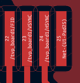
PCB 1.8, The pin 25 on U1 is connected to pin 98 on U2, pin 22 is unconnected.
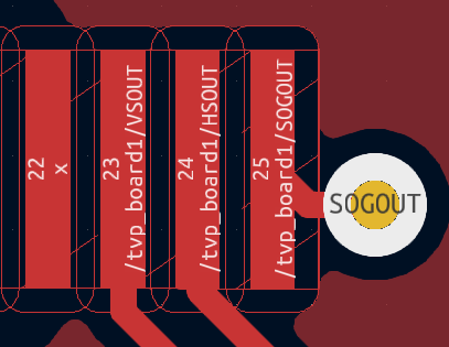
So for the convertion, on PCB 1.6 you need to lift the pin 22 on u1 (or cut the trace) and reconnect pin 25 on the path of pin 22.
-
This reply was modified 1 year ago by
-
This reply was modified 1 year ago by
July 3, 2024 at 8:33 AM #62244What cable you used (looks like a enameled one)?
It is enameled… but i don’t know the wire gauge. It’s probably AWG 30 or 31!? I don’t know for sure, because those are wire scraps from my former job, where colleagues used these kind of wires to manually wiring the components of in-ear hearing aids to each other.
-
This reply was modified 1 year ago by
-
AuthorPosts
- You must be logged in to reply to this topic.