v.1.7 not working even after JTAG flashing; how to debug?
NewHome › Forums › OSSC, OSSC Pro and DExx-vd isl › OSSC – DIY & Repair Support › v.1.7 not working even after JTAG flashing; how to debug?
- This topic has 10 replies, 2 voices, and was last updated April 29, 2025 at 12:02 PM by
spacesaver.
-
AuthorPosts
-
April 16, 2025 at 8:02 AM #65754
My v1.7 stopped working after the 3.5mm audio input cable touched the metal chassis of another power supply. Don’t know what that means. Maybe it caused static damage. I don’t think it would cause current flow, assuming the audio input has very high impedance.
LED back light is still on and I can reflash the 0.90-aud firmware with JTAG in Quartus Prime Programmer. But no text ever shows on the screen and the buttons don’t do any thing. Is there anything I can probe? I have a 1e9 sample/s oscilloscope.
April 16, 2025 at 6:06 PM #65757The FPGA may be okay if you’re able to flash it via JTAG Programmer… but you should check the 27Mhz oscillator and the voltage regulators.
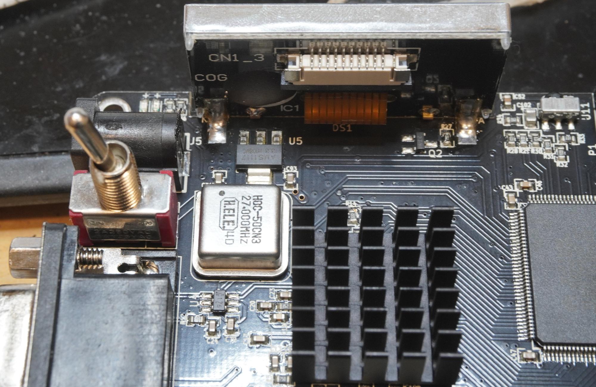
April 20, 2025 at 12:43 PM #65780Thanks for the tip. The oscillator is fine. All the regulators seem fine except U6
u5 3.3V # the ground pin is not the middle one like you said here https://videogameperfection.com/forums/topic/ossc-1-5-trouble/
u6 0.12V # the output pin has a ~1 ohm resistance to ground. Some kind of short?
u7 1.9
u9 1.8u12 1.2
u13 2.5
u14 1.2
u15 1.8
u16 1.8What could that mean?
April 20, 2025 at 10:44 PM #65781u5 3.3V # the ground pin is not the middle one like you said here
In the reference design it is! You can see it here – in the 3D rendering of the KiCAD file:

The middle pin is definitely connected to the ground plane.
BUT i’ve seen some modified PCB designs where other voltage regulators are used, which may have a very different pinout. Sadly i don’t know if your PCB follows the reference design.
u6 0.12V # the output pin has a ~1 ohm resistance to ground. Some kind of short?
U6 is a 3.3V regulator. There HAS to be something wrong (inside U6 itself or on its output line) if it only outputs 0.12V.
In short:
There’s definitely something wrong with (or with something connected to the output of) U6… and there may be something wrong with U5 (or with something connected to it… if your PCB uses the reference design). U5 is responsible for the supply voltage of U10 (the flash memory where the firmware is stored). It may(!) be possible, that U10 is damaged. I’ve seen one case, where U10 was broken and therefore its content was scrambled. Even though a JTAG update seemed to work, it was impossible to overwite its content… and since its content was gibberish the OSSC could not boot.April 21, 2025 at 2:32 AM #65782Hmm, on my OSSC 1.7, U5 is this regulator and the 3.3V output pin is the middle of the 3.
https://mm.digikey.com/Volume0/opasdata/d220001/medias/docus/5011/AMS1117.pdf
I don’t know how to tell if I have the reference design or a clone. I bought it in 10/2023 for $184 on eBay, so it seemed reputable.
Anyways, U5 is OK, as far as I can tell.
I checked VCC on the W25Q16JV flash chip and it is 3.3V. How can that be if you say U6 powers it?
Regardless, how about I connect the output of U5 to the output of U6 since you said they’re both 3.3V, and see if that fixes it?
 April 21, 2025 at 6:18 AM #65786
I don’t know how to tell if I have the reference design or a clone.
That’s not the reference design. U5 is rotated and it uses a different display with a flat flex cable connection, while the reference design uses this vertically mounted New Haven Display:
How can that be if you say U6 powers it?
I said: U5 powers it!
how about I connect the output of U5 to the output of U6 since you said they’re both 3.3V
I’m no electrical engineer… but there’s certainly a good reason for using two different regulators for the two 3.3V voltage rails. U5 drives the flash memory, the oscillator, the digital power (low noise) part of the audio ADC (U8) and the digital power (low noise) part of the TVP7002PZP (= U1 = the video ADC). U6 drives the analog power part of U1 and U8, and it drives U17 (the 3-Channel video buffer). Connecting U5 to everything U6 drives surely doubles its load. And while it may be able to withstand it, it could introduce noise to the digital power part of both ADCs AND there may be a broken component on the output line of U6 (while U6 itself is NOT broken)… which could subsequently kill U5 (and/or components connected to it) or at least damage your OSSC further.
Your OSSC does not use the reference design – that’s why it’s hard to tell, which voltage regulators are swapped for cheaper or more readily available parts. So i would not stress them any more than necessary. First: look if U6 itself is broken (= remove it and see it the short is gone)… if it is: look if it’s a TLV70033 (the markings can give a clue) and find a replacement.
April 21, 2025 at 8:21 AM #65787This guy also had a broken U6 regulator. https://videogameperfection.com/forums/topic/trying-to-repair-a-dead-ossc-u6-and-u1-were-replaced-boots-but-no-test-pattern/
Aha, I know 1 thing that’s broken for sure: the PCM1862 ADC (U8). I injected 3.3V externally through the U6 regulator output pin and it draws ~10A ! I touched all the chips that it powers and only U8 got hot. U1 is hard to tell because it’s so big and will take a long time to heat. That makes sense U8 got damaged, assuming that’s what the analog audio input connects to – I see pins named I2S in ossc_board.pdf, so that means audio.
This seems to be a case of permanent latchup. I’ve seen many microcontrollers ruined by latchup, presumably from applying signals before power, causing the gate voltage to exceed VDD.
Before I replace components, is it expected for the firmware to not print anything on the LCD? Does it mean it’s stuck forever reading/writing I2C and not getting a response?
April 21, 2025 at 11:03 AM #65788is it expected for the firmware to not print anything on the LCD?
The firmware is able to print out “init error” messages on the LCD if some of the ICs are not responding:
But not for every IC… and only if they are not responding. An IC causing a short on one of the power rails may result in a more unpredictable behaviour. But still: no output at all on the LCD is (at least) strange. I’ve seen a case of a broken oscillator and another case of a broken flash memory causing it… but i’ve never seen a broken audio ADC as the culprit.
You may simply try to remove U8… to see, if the short is gone… and to check, if U6 outputs 3.3V without it. You may get the LCD output back without it – but if you don’t, there may be something else damaged too.
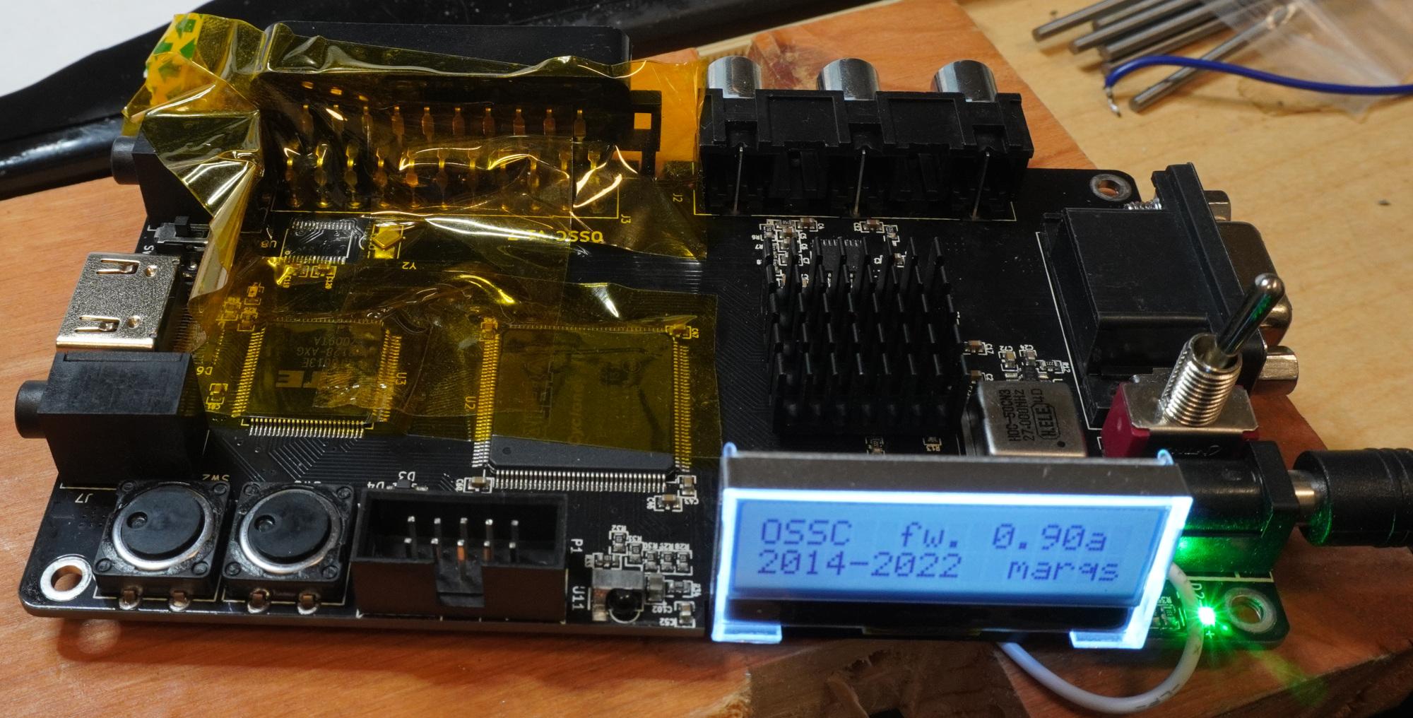
April 23, 2025 at 7:03 AM #65807Hurray! it’s back after desoldering the audio ADC. I got no HDMI output at 1st because the U6 regulator was damaged and only outputting 1.7V. I fed U5 into U6 and got HDMI to work. I noticed the VGA signal was noisy around sharp edges, which is what you warned since analog power is supposed to be separate from noisy digital ones.
Very glad this unit was saved. Thank you very much Morpheus for the insights. Someone should check if the I2C code for the ADC will hang forever if the clock is pulled low indefinitely. I didn’t get to check before I desoldered.
 April 23, 2025 at 8:50 PM #65813
Nice to see your OSSC back alive and (considering all the circumstances with the damaged U8 and U6) relatively well. Luckily those two aren’t the most expensive parts.
That’s one of the great things with the OSSC: its good repairability!
April 29, 2025 at 12:02 PM #65875Hurray again. Audio input is back now. The replacement ADC and LDO regulator arrived from DigiKey today and I’ve installed them. I had a difficult time aligning the pins for soldering. I even ripped 1 of the traces when trying to realign, but miraculously, it was the IOVDD line, which can be shared with DVDD next to it.
-
AuthorPosts
- You must be logged in to reply to this topic.