DIY Guides, Howto & Guides
Sega MegaDrive 1 RGB Bypass Installation Guide (updated 7/1/19)
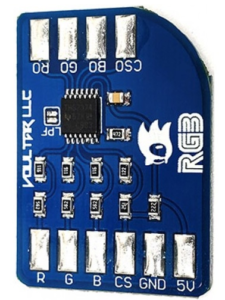
The long awaited Megadrive RGB bypass board by Voultar is now available in our store, both for DIY installers and as a fitted part. Big thanks to Voultar for this open source design and for allowing us to sell the board on our site.
Fitting the RGB bypass amp is a little more complicated than we had anticipated. However, our friends over at BetaGamma Computing have come to the rescue with this handy guide (also available in PDF format here).
Without further delay, let’s hand over to BetaGamma Computing for the install guide.
This step by step guide describes the Installation of the open source Voultar RGB Bypass Amplifier board for the original SEGA MegaDrive/Genesis 1.
A Megadrive/Genesis board revision BD M5 PAL has been used in this document but the procedure is virtually the same for other revisions as well as for NTSC Models. Minor differences that may occur are the locations of the pure RGB and CSYNC signals obtained from the video processor chip.
Scope of Installation
The MegaDrive 1 is a fantastic console but it is sadly plagued by a soft RGB output often with horrendous jailbars. Various methods exist to mitigate the jailbar effect, but only a bypass amp such as this one can eliminate them completely (very minor traces may remain on some consoles when subjected to intense scrutiny).
This modification removes the onboard CXA-1145 from all RGB video processing functions. It does this by isolating all input and output signals to and from the CXA-1145, picking up the RGB and CSYNC source signals as close to the VDP as possible. It also removes any tracks carrying these signals on the PCB. These are no longer required and removing them will avoid them picking up noise.
The 8 PIN DIN Connector on the Mega Drive is configured to use a Scart cable that is wired for clean CSYNC on Pin 7. Composite video for sync cables are not compatible as composite video will not be generated by the console after this Installation.
It is advised that a competent engineer performs this modification for you. If you don’t feel confident after reviewing this guide then use VideoGamePerfection.com’s fitting service.
Revision 1 board only – Add pull up resistor
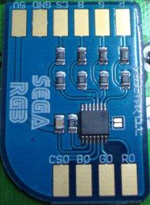
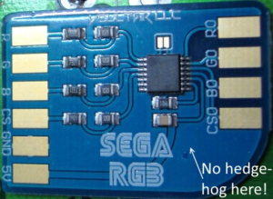
If your RGB bypass board is a revision one model, then you should add an extra resistor to the board. If your board does NOT have a small hedgehog head on it, then it is a revision 1.
CSYNC output from the VDP requires a 2k2 pull up resistor in order to feed the CXA or Bypass board correctly. The original circuitry on the motherboard uses a 2k2 resistor but due to the way we isolate CSYNC from the VDP we are unable to include this important component hence we need to re-introduce it on our Bypass installation.
Revision 2 Boards have this 2k2 resistor added to the Bypass board and do NOT require this fix.
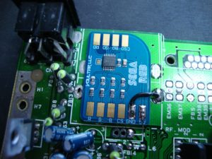
You can use any 2k2 resistor, size permitting, as long as it is of good quality. A metal film resistor with a low tolerance for example. Wattage value is not important in this application. Connect this 2k2 resistor between the +5V and CS Pads on the input side of the Bypass amplifier.
In the above example, @Consoles4You has added an SMD type 2k2 resistor.
Installation
Disconnect all power from your console and carefully strip the unit down, noting which screws came from where and keep them safe. Remove the mainboard from the casing and place on an anti-static protected workbench.
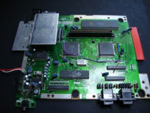
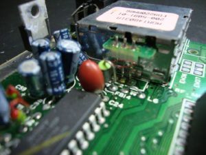
The above picture shows our stock unmodified console. First we need to carry out some steps to prepare it for the new amplifier PCB.
There are 2 screws thermally fixing the 2 voltage regulators to the heatsink seen in the top left of the picture. Carefully remove these screws, then also remove the 2 heatsink mounting screws from the solder side of the board. These 4 screws MUST only be used to re-fix the heatsink later.
You should now be able to carefully lift away the heatsink, giving full access to the video encoder circuitry.
Now we need to remove the RF modulator. The RF modulator will no longer be functional after the Installation and removing it will provide a great area for mounting the new PCB with the added bonus of a grounding plane providing extra noise shielding.
See the picture below and carefully snip the 3 signal lines as circled, this makes it easier to remove the RF Modulator.
You will need a higher wattage soldering iron to remove the RF modulator by carefully flowing the solder at its three mounting points on the solder side of the board.
Gently rock the modulator away from the board by going around the three solder points in turn repeatedly.
Once the modulator has been removed you can turn your attention to the 3 snipped connection points which can now be easily de-soldered and removed.
Finally, use some solder wick and IPA to remove any excess solder and flux from both sides of the board.
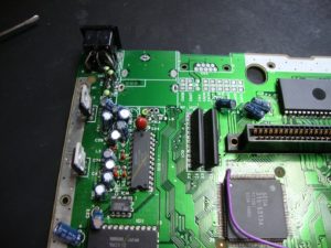
Your main board should now look like the picture shown below.
The next step is to locate the VDP RGB and CSYNC source signals.
On the BD M5 PAL board the signals we need are located to the west of the chip and circled in the above picture.
Different boards may have slightly different tracking or location but they will all be similar.
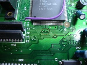
The 315-5313 – YM-7101 VDP carries the signals on the following pins, refer to Internet Wiki’s for other device variants.
RED – PIN 27
GREEN – PIN 28
BLUE – PIN 29
CSYNC – PIN 42
From the picture above you can easily identify that the 3 grouped pads are RGB left to right and the solitary pad is CSYNC.
Using a scalpel, carefully scrape away the top green PCB lacquer of the 4 Identified pads until the copper is exposed. Be careful not to cut anything.
Now, use IPA to wash away any dust and clean the copper, then carefully tin all 4 exposed pads with a little solder.
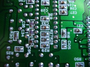
Now it’s time to turn the board over to the solder side and make some track modifications to isolate the signals.
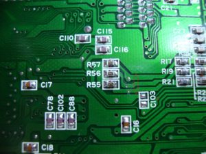
R55, R56, R57 are pull up resistors which help protect the VDP RGB outputs so it is beneficial to leave them in circuit.
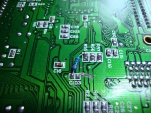
We need to cut a total of 4 tracks as circled in red above. Use a scalpel, take care and take your time.
I would advise carrying out continuity checks to ensure the track cuts are successful.
Due to the way the PCB is laid out and for us to obtain the best noise free isolation we have to discard the mainboards pull-up resistor for the CSYNC signal and install our own.
Using a ¼ Watt or smaller 2k2 resistor cut and solder it as shown below.
Locate Pin 10 of the CXA1145 on the solder side and cut the track as shown below.
The use of continuity checking is advised to ensure isolation.
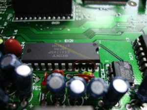
The next step is to cut 4 pins away from the CXA1145 IC. Use fine tipped cutters and cut the pins as they emerge from the housing, see the picture below.
You will need to cut and isolate Pins 21, 22, 23, 10.
Once you have cut the 4 pins you can desolder the 4 chip legs and remove them completely, clear the 4 PCB holes from solder ready to insert new wiring.
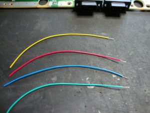
Cut 4 x 80CM lengths of appropriately coloured multi-strand wires, strip and tin the ends as shown.
Now it’s time to mount the new amplifier PCB. See the following picture for the location, ensure the PCB surface is degreased with IPA first and there are no existing solder ridges in place.
Peel away the cover on the double sided tape behind the amplifier and affix in place.
This location conveniently keeps us away from digital signal processing as well as providing a very convenient power supply for our new amplifier.
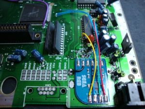
You can use the leftover lead from the resistor used earlier, carefully bend so it remains isolated, to hookup the +5V supply as shown.
A short run of insulated wire can be installed for the ground as shown.
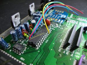
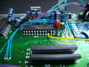
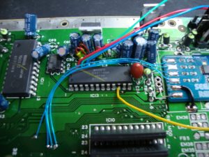
Using our four prepared coloured wires, Install them into the vacant PCB holes alongside the CXA1145 as shown.
The pinout is as follows:-
RED – PIN 23
GREEN – PIN 22
BLUE – PIN 21
CSYNC – PIN 10
Take care to run the Insulation right up to the PCB surface to ensure no electrical contact is made to the CXA in any way.
The other end of these cables will connect to the amplifier outputs later on in the Installation, for now just leave them be.
Now it is time to hook up the VDP signals to the amplifier PCB. Simply connect RGB and CSYNC, from the VDP pads we prepared on the mainboard earlier, to the 4 corresponding pads on the Input side of the amplifier PCB.
I recommend the use of AWG 30 Kynar wire. Pre tin the ends before soldering to the VDP pads.
Careful routing of these 4 signal wires is of ultra Importance. These wires are prone to picking up noise from the mainboard digital processing systems.
For best results, follow the path as pictured and leave a gap between the PCB surface and wires.
At this point you should decide if you want the low pass filter on or off. Most people leave this filter off though there is considerable debate as to what is the best option for this and no clear right or wrong answer. Many people believe that if you’re using the console predominantly with a scaler like the OSSC or XRGB Mini you should disable or turn off the low pass filter, otherwise you should leave it on. Turning off the filter can give a slightly sharper image but can also introduce other problems, such as picture noise.
If you want to enable the low pass filter, use a small blob of solder now to close the filter option jumper on the amplifier PCB.
Once all 4 signal source wires have been installed, clean the flux away from all solder points using IPA.
The final step is to cut to size and solder the 4 coloured cables we installed earlier into the CXA vacant PCB holes. These should be soldered on to the amplifier PCB following the R-G-B and SYNC identification.
Double check all your work at this point and perform final cleaning.
You can hook up your console now to test the modification. Please ensure you do not run it for more than 30-40 seconds without the heatsink refitted as the regulators will overheat.
If the test goes successfully then rebuild your console by reversing the way you stripped it down and enjoy your new enhanced video output quality.
Configuring your RGB SCART cable
A RGB bypassed console requires the use of a RGB cable wired for composite sync (CSYNC). It cannot be used with a cable wired for composite video for sync.
A typically configured RGB SCART cable for the Sega Megadrive should have a 470ohm resistor on the CSYNC line of the cable along with a 220uF cap.
Bas Gialopsos – BetaGamma Computing January 2019







Hi,
I’m trying to get hold of a PC engine ifu-rgb board from Voultar, is this something you could get a hold of?
Sorry no, we haven’t been able to 🙁
On USA VA3 with rev 2 bypass is it still necessary to add the 2k2 resistor from CSYNC to R55? I noticed there’s a resistor in Circuit on the VA3 already.
Hi there, I am using a VA4 PAL European board. In regards to your question about lifting the pins directly, according to this photo you can https://twitter.com/ifixretro/status/1027399360160714752 my understanding as per the instructions above is that there are extra resistors on the board that provide protection.
“R55, R56, R57 are pull up resistors which help protect the VDP RGB outputs so it is beneficial to leave them in circuit.”
Good luck = )
I have been checking for this every month for the past two years! beyond excited to get this finally = )
Which console model, and install method do you plan on using?
Hi Matt, really sorry for duplicate posts… I’m not seeing my previous comments being posted but now I’m logged in so trying one last time.
I have a Japanese model 1 VA4. Is the installation method described above still recommended for my console too? I ask because I’m reading conflicting results and install methods where others are lifting R,G,B,CSYNC pins on the VDP and getting the signals directly from there instead of cutting tracks and adding a resistor on the mainboard.
Thanks!
Not sure sorry. Our forum would be the best place for these questions but I can’t guarantee an answer.
Hi Matt. Is it possible to install this board using the other method of lifting the R,G,B,CSYNC pins on the VDP and getting the signals directly from there instead of cutting the tracks on the mainboard and adding a resistor for CSYNC?
I’d like to install this into a Japanese model 1 VA4.
Thanks
Any instructions for a pathetic Sega Master System 1?
Ive just put together this on my PAL Mega Drive and the results are fantastic through the OSSC, however, doesnt work through my Framemeister ‘NO_INPUT’. Do i need to remove a resistor from my scart cable? And if so what pin? New to all this so im still learning….
Yes I think that’s probably the case. I’m actually looking into that myself at the moment.
Will this work with a model 2 with the Samsung chip? I’d just be happier not using that chip for my video and I cant seem to find an Install guide anywhere!
As far as I’m aware these are for Model 1 Genesis consoles only.
I thought his original Twitter post this new board would work on all consoles?
after installation i can use a cable with no caps or resistors on the scart end?
leave the caps but remove the resistor from CSYNC.No, please use a standard Megadrive RGB SCART cable with all normal caps and resistors.