Morpheus_79
@morpheus_79
Forum Replies Created
-
AuthorPosts
-
Afaik: up until OSSC 1.6 D5 is for protective/ESD reasons. It delivers an alternative electrical path – for example: if you use a power supply with the wrong polarity.
D5 (SD05-7) is rated for a working voltage of 5V:
… so the 9V most definitely killed it. Your OSSC should work fine without it… but i would recommend to replace it with the same or a similar diode.
Afaik the video output of almost all VCRs has a very (VERY!) unstable sync signal. CRT TVs can cope with it easily – but it’s a big problem for all ADCs. It’s a technical issue and a result of the way VCRs work. There are minimal speed fluctuations for the motor… worn VHS tapes are more stretched in the areas that have been watched more frequently -> all this causes an unstable sync signal, which gets even worse for Longplay-Recordings.
I remember the later days of VHS-Capturing: there were recommendations for using VHS/DVR combo player/recorder, because some had an integrated TBC:
https://en.wikipedia.org/wiki/Time_base_correction
For VHS without a TBC it’s kind of a gamble on how stable the digital output from an ADC looks: it may be okay for one tape… but with another tape you have lots of flickering caused by lost sync.
What value is R36 and what are the specs if I need to buy the part online.
According to the official BOM R35 and R36 are 330 ohm resistors:
https://github.com/marqs85/ossc_pcb/tree/v1.6/bom
They are both current limiting resistors -> one for each LED:
https://www.build-electronic-circuits.com/current-limiting-resistor/
Is the top pad on R35 needed or can I just solder the wire to the bottom pad and go from there?
The wire needs to be soldered to the pad connected to the Cyclone IV FPGA (U2). The other pad is connected to the LED. I don’t know if on your Chinese OSSC the top or bottom pad connects to the FPGA -> but the wire HAS TO BE connected to the correct pad… otherwise the mod won’t work!
What is the best way to clean up the mess on the IC?
Solder wick???
What is the easiest way to connect the heatsink to the IC?
There’s thermally conductive (epoxy) glue for (permanently) mounting a heat sink onto an integrated circuit. If you want a reversible solution: there’s also thermally conductive adhesive tape. Keep in mind: you need thermally conductive stuff -> regular glue and regular adhesive tape WON’T WORK!!!
April 26, 2025 at 11:24 AM in reply to: Overvolted OSSC 1.6 has no input nor output [updated] #65837I think my multimeter can measure Hz (I don’t know to which extent, and if it can help)
It’s an 27Mhz oscillator. While your multimeter may have some oscilloscope features, such additional functionalities are mostly rudimentary and limited to a kHz range.
Do you have an idea how much it will cost ?
Sadly i don’t know. The repair may be cheap in replacement parts… but the final cost highly depends on the invested time and complexity for the fault finding and repairing.
Since C18 is a decoupling capacitor for the (by U6 delivered) 3.3V supply of the analog part of U1, it may be possible that U1 is at least partially broken. There would be a “Init error -3” message on the LCD if U1 does not respond at all – but since there is no message, a partially damaged TVP7002 is still possible.
A partially broken U1 would explain the “NO SYNC” message. But it does not explain the missing test pattern, since the FPGA outputs the test pattern istself, without needing the video ADC for it. A shorted clock line may be possible – but there was a pretty new thread in here, where someone had a broken oscillator… which resulted in no LCD output at all. So i would assume: the (main) clock signal is pretty much needed for everything to work properly. A missing/shorted clock would result in the OSSC not doing anything at all. But if you have an oscilloscope, you could check if the oscillator outputs a stable clock.
The same 3.3V line that drives the analog part of U1 drives the analog part of U8 too. U8 delivers the digitized audio to the HDMI transmitter (U3). So it may be possible, that (because of a short in that line or from an overvoltage) U8 was damaged too and sends some I2S-data-garbage to U3, that confuses it… resulting in U3 not working properly.
That’s just an educated guess… but you can test it by removing U8. If this does not give you the test pattern, U3 may be damaged. It is driven by a different 3.3V line (from U5) – but it’s hard to tell what voltage U5 delivered after powering it with the out-of-specs 9V…Btw… the shorted C18 is kind of strange, since common 0603 ceramic capacitors are rated for 16V or even more (the official BOM uses a 16V rated capacitor) – 9V would not do them any harm (there are 6.5V ceramic caps available, but because of the DC bias effect it makes no sense to use them in 5V systems). So there could be another reason than just “i accidentally powered it with 9V” behind the damage of this broken OSSC…
April 23, 2025 at 8:50 PM in reply to: v.1.7 not working even after JTAG flashing; how to debug? #65813Nice to see your OSSC back alive and (considering all the circumstances with the damaged U8 and U6) relatively well. Luckily those two aren’t the most expensive parts.
That’s one of the great things with the OSSC: its good repairability!
April 21, 2025 at 11:03 AM in reply to: v.1.7 not working even after JTAG flashing; how to debug? #65788is it expected for the firmware to not print anything on the LCD?
The firmware is able to print out “init error” messages on the LCD if some of the ICs are not responding:
But not for every IC… and only if they are not responding. An IC causing a short on one of the power rails may result in a more unpredictable behaviour. But still: no output at all on the LCD is (at least) strange. I’ve seen a case of a broken oscillator and another case of a broken flash memory causing it… but i’ve never seen a broken audio ADC as the culprit.
You may simply try to remove U8… to see, if the short is gone… and to check, if U6 outputs 3.3V without it. You may get the LCD output back without it – but if you don’t, there may be something else damaged too.
April 21, 2025 at 6:18 AM in reply to: v.1.7 not working even after JTAG flashing; how to debug? #65786I don’t know how to tell if I have the reference design or a clone.
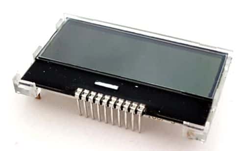
That’s not the reference design. U5 is rotated and it uses a different display with a flat flex cable connection, while the reference design uses this vertically mounted New Haven Display:
How can that be if you say U6 powers it?
I said: U5 powers it!
how about I connect the output of U5 to the output of U6 since you said they’re both 3.3V
I’m no electrical engineer… but there’s certainly a good reason for using two different regulators for the two 3.3V voltage rails. U5 drives the flash memory, the oscillator, the digital power (low noise) part of the audio ADC (U8) and the digital power (low noise) part of the TVP7002PZP (= U1 = the video ADC). U6 drives the analog power part of U1 and U8, and it drives U17 (the 3-Channel video buffer). Connecting U5 to everything U6 drives surely doubles its load. And while it may be able to withstand it, it could introduce noise to the digital power part of both ADCs AND there may be a broken component on the output line of U6 (while U6 itself is NOT broken)… which could subsequently kill U5 (and/or components connected to it) or at least damage your OSSC further.
Your OSSC does not use the reference design – that’s why it’s hard to tell, which voltage regulators are swapped for cheaper or more readily available parts. So i would not stress them any more than necessary. First: look if U6 itself is broken (= remove it and see it the short is gone)… if it is: look if it’s a TLV70033 (the markings can give a clue) and find a replacement.
April 20, 2025 at 10:44 PM in reply to: v.1.7 not working even after JTAG flashing; how to debug? #65781u5 3.3V # the ground pin is not the middle one like you said here
In the reference design it is! You can see it here – in the 3D rendering of the KiCAD file:

The middle pin is definitely connected to the ground plane.
BUT i’ve seen some modified PCB designs where other voltage regulators are used, which may have a very different pinout. Sadly i don’t know if your PCB follows the reference design.
u6 0.12V # the output pin has a ~1 ohm resistance to ground. Some kind of short?
U6 is a 3.3V regulator. There HAS to be something wrong (inside U6 itself or on its output line) if it only outputs 0.12V.
In short:
There’s definitely something wrong with (or with something connected to the output of) U6… and there may be something wrong with U5 (or with something connected to it… if your PCB uses the reference design). U5 is responsible for the supply voltage of U10 (the flash memory where the firmware is stored). It may(!) be possible, that U10 is damaged. I’ve seen one case, where U10 was broken and therefore its content was scrambled. Even though a JTAG update seemed to work, it was impossible to overwite its content… and since its content was gibberish the OSSC could not boot.April 16, 2025 at 6:06 PM in reply to: v.1.7 not working even after JTAG flashing; how to debug? #65757The FPGA may be okay if you’re able to flash it via JTAG Programmer… but you should check the 27Mhz oscillator and the voltage regulators.
Strange behaviour. Maybe a problem with U5 (AP7361C-33E-13)??? It’s the voltage regulator responsible for creating the needed 3.3V out of the supplied 5V. But then: there’s the ‘as soon as I moved it…’ part, which sounds odd. Maybe there’s a (half) broken capacitor creating some problems? You could use a plastic spudger or pen and poke a bit around on some of the caps…
No. Why? You can try to replace the THS7353 (U17). It’s available from LCSC, Mouser, DigiKey and other suppliers:
https://www.lcsc.com/product-detail/Video-Amplifiers_Texas-Instruments-THS7353PWR_C2652733.html
https://mou.sr/43rSQvO
https://www.digikey.com/short/n19p40zd… and costs around 5 bucks. If you don’t know how to replace it yourself, you can try to give it to someone who does (a friend or a repair shop).
As ‘marqs’ said: there could be something else broken… but it’s a good starting point and it doesn’t cost the earth.
-
This reply was modified 1 year, 3 months ago by
Morpheus_79.
I would recommend reverting back to the last firmware version that worked. Especially if you don’t need any feature of the newer versions.
Since the OSSC Pro is a scaler it has way better compatibility with TVs (resolution wise). It also should be more stable with the more “exotic” outputs of some retro gaming consoles and it comes with sophisticated deinterlacing methods for interlaced video input.
So all in all the OSSC Pro is the better solution – but i’m not sure, if it’s worth buying just for SNES upscaling and nothing else…
We need more information:
Which board revision of the OSSC do you have (1.8 or older)? If it’s an older revision than 1.8: is it modded for the use of the v1.xx firmwares as described here(?):
I forgot…
According to @marqs :
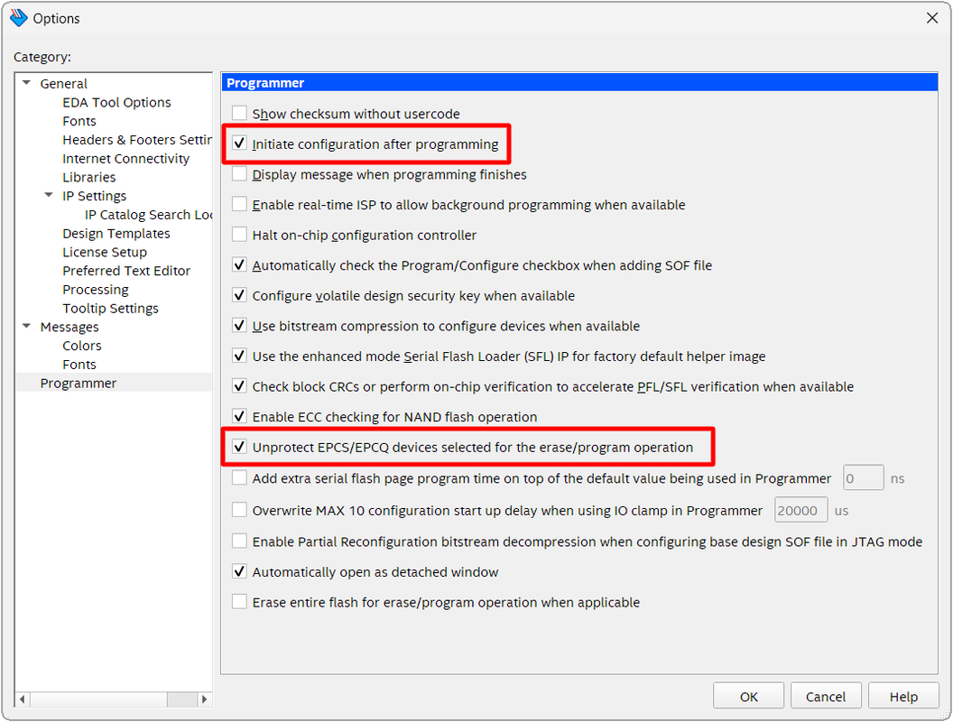
To program flash, a combined FPGA image must be first generated and converted into JTAG indirect Configuration file (.jic). Open conversion tool (“File->Convert Programming Files”) in Quartus, click “Open Conversion Setup Data”, select “ossc_pro.cof” and press Generate. Then open Programmer and ensure that “Initiate configuration after programming” and “Unprotect EPCS/EPCQ devices selected for Erase/Program operation” are checked in Tools->Options. Then clear file list, add generated file (output_files/ossc_pro.jic) and press Start after which flash is programmed. Installed/updated firmware is activated when programming finishes (or after power-cycling the board in case of a fresh flash chip).
… both of these checkboxes should be ticked:
-
This reply was modified 1 year, 3 months ago by
-
AuthorPosts